
The Belgian microelectronics research center imec, together with AIXTRON, GlobalFoundries, KLA, Synopsys, and Veeco, has become the first research partners in its 12-inch gallium nitride (GaN) open innovation research project, focusing on low-voltage and high-voltage power electronic component applications.
Imec stated that its research with partners is part of the imec Gallium Nitride Power Device Industry Alliance (IIAP) program, with the goal of developing 12-inch gallium nitride epitaxial growth and high-voltage and low-voltage gallium nitride high electron mobility transistor (HEMT) process flows. Using a 12-inch substrate will not only reduce the manufacturing cost of gallium nitride devices, but will also enable the development of more advanced power electronic devices in the future, such as high-efficiency low-point-of-load (POL) converters for CPUs and GPUs.
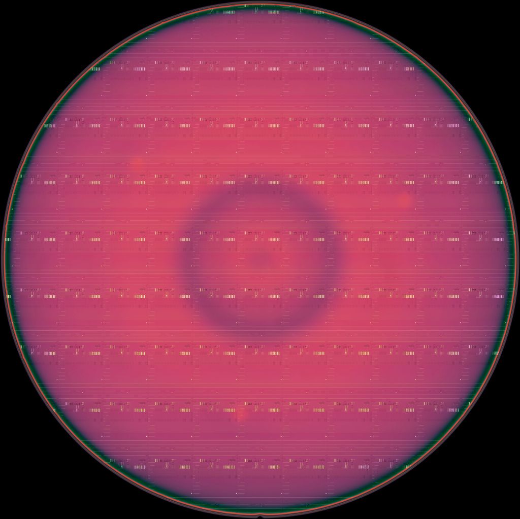
The 12-inch gallium nitride on silicon wafers supplied by AIXTRON were inspected on the 8-series/CIRCL tools provided by KLA after p-type gallium nitride etching was completed at imec.
The increasing demand for gallium nitride (GaN) fast chargers highlights the development potential of GaN technology in power electronics applications. Backed by continuous advancements in GaN epitaxial growth, GaN device and wafer manufacturing, reliability and robustness, and system-level optimization, GaN technology is poised to enable a new generation of power electronics. These products will enter the market with smaller form factors, lighter weight, and superior energy conversion efficiency compared to silicon-based solutions. Examples include automotive onboard chargers and DC/DC switches, solar panel inverters, and power distribution systems in telecommunications and AI data centers—GaN-based components in these applications contribute to the comprehensive decarbonization, electrification, and digitalization of society.
A clear trend in gallium nitride (GaN) technology development is the shift to larger wafer sizes, with most available capacity currently at 8-inch wafers. With imec proposing a 12-inch GaN research direction, imec is now taking the next step, building on its 8-inch wafer expertise. Stefaan Decoutere, Imec Technical Fellow and head of the GaN Power Electronics Research Program, stated that the benefits of switching to 12-inch wafers go beyond simply increasing production scale and reducing manufacturing costs. "Our CMOS-compatible GaN technology is now available in cutting-edge 12-inch devices, which will allow us to develop more advanced GaN power devices. For example, ultra-miniaturized low-voltage p-type GaN gate HEMTs for POL converters contribute to high-energy-efficiency power distribution in CPU and GPU applications."
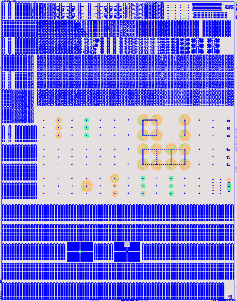
A photomask assembly for the development of gallium nitride (GaN) high electron mobility transistors (HEMTs) using a 12-inch substrate.
As part of the 12-inch gallium nitride (GaN) research program, the first step will be to establish a baseline lateral p-type GaN HEMT technology platform, targeting low-voltage applications such as 100V, using 12-inch silicon (111) material as the substrate. To this end, a process module primarily based on p-type GaN etching and ohmic contact forming is currently under research. Following this, the focus will shift to high-voltage applications. For applications above 650V, development will utilize a 12-inch SEMI-compliant and CMOS-compatible QST substrate (containing a polycrystalline aluminum nitride core layer). During these development phases, controlling the curvature and mechanical strength of the 12-inch wafer is a primary consideration.
This 12-inch gallium nitride (GaN) research initiative follows the successful completion of 12-inch wafer fabrication testing and photomask development. Imec aims to complete all 12-inch wafer capacity setup in its 12-inch cleanroom by the end of 2025. Stefaan Decoutere emphasized that the success of 12-inch GaN development also relies on the ability to build a robust ecosystem and collectively drive innovation, encompassing everything from 12-inch GaN growth and process integration to packaging solutions. Therefore, we are pleased to announce Aixtron, GlobalFoundries, KLA-Tex, Synopsys, and WEC Instruments as our initial research partners for the 12-inch GaN open research program, and we hope to welcome more partners soon. Developing advanced GaN power electronics requires close integration between design, epitaxy, process integration, and applications—a connection whose crucial role has been proven in our forward-looking research on 8-inch GaN.
(Image source: imec)


