In recent years, a number of domestic LED companies have been actively promoting the development of Micro LED technology through various means such as technology research and development, capacity building, and capital injection. The performance of Micro LED has been rapidly improved, and its application scope has been continuously expanding from large-size displays, automotive displays, and near-eye displays.
At the ongoing SID 2025 exhibition in the United States, several Chinese companies went to the exhibition site to showcase the latest progress of their Micro LED technology to the overseas market, demonstrating China's strength in Micro LED.
Overseas, a large number of companies are also working hard to promote the development of Micro LED related technologies. Just recently, three international manufacturers reported the latest financing, orders, and technological progress in their Micro LED businesses, involving the development of Micro LED interconnect technology, Micro LED wafers, and nanowire Micro LED technology.
Avicena Raises $65 Million in Funding to Drive Micro LED Chip Interconnect Technology to Market <br /> Avicena, a US-based developer of Micro LED-based chip optical interconnect technology, recently announced the completion of its Series B funding round, raising $65 million (approximately RMB 469 million). Avicena will use the funds to further expand its team and advance its first product into mass production. With this latest round of funding, Avicena has now raised a total of $120 million.
Avicena is dedicated to developing LightBundle™, an ultra-low-energy optical link technology based on Micro LEDs. This technology is based on highly parallel optical interconnects created by densely packed GaN-based Micro LEDs, which can be integrated onto all high-performance CMOS integrated circuits, offering high bandwidth density and energy efficiency.

How LightBundle™ works (Image source: Avicena)
Compared to traditional copper link technologies, LightBundle™ link technology offers advantages such as low power consumption, low latency, wide coverage, and high bandwidth density. Therefore, LightBundle™ link technology can be applied to interconnects between high-performance computing (HPC) systems, artificial intelligence (AI)/machine learning (ML) and discrete memory chips, as well as next-generation link applications such as sensors, 5G wireless, and aerospace.
In recent years, Avicena has actively promoted the development of LightBundle™, a Micro LED chip interconnect technology, through acquisitions and collaborations.
In 2022, Avicena acquired Nanosys' GaN-based Micro LED manufacturing plant and related engineering team from the US quantum dot light-emitting materials and technology supplier to further enhance its R&D and production capabilities in LightBundle™ technology.
In 2023, Avicena partnered with ams OSRAM to jointly promote the mass production of LightBundle™ technology.
Recently, Avicena further enhanced its LightBundle™ technology by launching a scalable and modular LightBundle interconnect platform that supports transmission capabilities of over 1Tbps/mm and can extend ultra-high-density chip-to-chip (D2D) interconnect distances to over 10 meters at low energy efficiency levels.
Compound semiconductor foundry IQE sees increased Micro LED wafer orders . Recently, UK-based compound semiconductor foundry IQE released its 2024 results. In 2024, IQE achieved revenue growth, reaching £118 million (approximately RMB 1.129 billion), a year-on-year increase of 2.4%; and adjusted EBITDA of £8.1 million, a year-on-year increase of 88.1%.
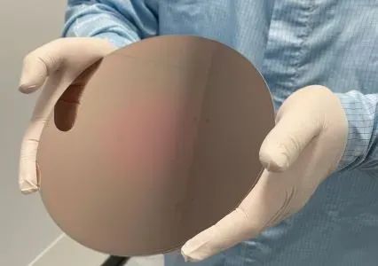
Image source: IQE
In its earnings report, IQE mentioned that the company has extended its partnership with an AR smart glasses design company and secured an annual purchase order commitment based on gallium nitride Micro LED display technology.
In addition, IQE stated that it has launched an 8-inch GaN-on-Si (gallium nitride silicon) Micro LED foundry service, equipped with an internal wafer cleaning process and compatible with silicon-based CMOS processes.
IQE is an independent outsourcing manufacturer that manufactures epitaxial wafers based on metal-organic vapor deposition, molecular beam epitaxy, and chemical vapor deposition. IQE's products cover compound semiconductor epitaxial wafers such as GaN and GaAs.
In response to the demand for Micro LED in the AR glasses field, in recent years, IQE has successively provided the ability to mass-produce Micro LEDs with MICLEDI, a fabless manufacturer of Micro LEDs for AR, and has also reached a cooperation with Porotech, a UK Micro LED technology manufacturer.
Aledia to Offer 3D Nanowire Micro LED Wafer Samples in Second Half of This Year <br /> French 3D structure GaN LED technology developer Aledia announced that it will launch its new, mass-producible FlexiNOVA epitaxial wafer platform in the second half of this year and provide customers with the first samples, covering both 6V and 9V models.
FlexiNOVA's Micro LED wafers will be supplied to display manufacturers for integration into complete displays, targeting applications including wearable devices, automotive displays, televisions, and monitors. The FlexiNOVA platform reportedly offers high flexibility in chip size, shape, and power consumption.
Aledia states that a key innovation of FlexiNOVA lies in its ability to manufacture ultra-small chips, ranging in size from 15×30µm² to less than 3.5×3.5µm², on 8-inch gallium nitride silicon-based wafers. Feasibility of scaling up to 12-inch wafers has also been demonstrated. FlexiNOVA is also the first chip format to support built-in multi-voltages, reducing current density and alleviating electrical stress on the thin-film transistor (TFT) backplane, thereby improving thermal management and durability in automotive and battery-powered devices.

Image source: Aledia
Aledia has been dedicated to the research and development of 3D structure GaN Micro LED technology, also known as nanowire technology.
This technology creates LEDs through a nanoscale columnar three-dimensional processing on a wafer. These LEDs offer higher brightness and can achieve full-color displays by adjusting the nanowire structure. Aledia's Micro LED products can be used in various display products.
In 2023, Aledia completed a financing round of €120 million (approximately RMB 924 million) to mass-produce its Micro LED products. In 2024, Aledia developed what it claimed to be the world's most efficient 1.5μm Micro LED, with an external quantum efficiency (EQE) of over 32%, achieving a photoelectric conversion efficiency (WPE) of 320 milliwatts of visible light output per watt of electrical power.
summary
Micro LED technology is undergoing frequent developments, with domestic and international companies vying for dominance in the field, driving its advancement towards higher performance and wider applications. In the future, Micro LED is expected to play a significant role in displays and many other fields.


