Recently, a South Korean research team demonstrated a new technology that is expected to significantly improve the repair accuracy of Micro LEDs—Femtosecond Laser-Induced Breakdown Spectroscopy (fs-LIBS)—and published their findings in Scientific Reports.

Image source: Scientific Reports
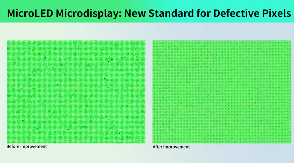
It is understood that with the popularization of ultra-high resolution displays such as 4K and 8K, a single panel may contain more than 20 million RGB sub-pixels, so any tiny flaw can affect the display quality. How to accurately remove flawed chips without damaging surrounding circuitry has become a major bottleneck in mass production.
The research team stated that traditional laser repair techniques cannot determine the "depth of the cut" in real time, which can easily damage nearby microelectrodes or thin-film transistors when repairing defects. The new research utilizes fs-LIBS technology, allowing the laser to "see" changes in material composition while processing, essentially providing built-in depth detection capabilities and improving repair safety.
The team used a Micro LED sample only 2.7 micrometers thick, containing a multi-layered structure of gold (Au), aluminum (Al), and gallium arsenide (GaAs). The experiment employed femtosecond lasers for micro-ablation, simultaneously measuring the plasma spectrum to determine the material layers from the spectral signals. The results showed that only a few laser pulses were needed to clearly detect the spectral lines of gold and gallium, and the increase or decrease in their signals precisely corresponded to the interface between the electrode layer and the LED functional layer.
At optimal laser energy, the team was able to remove only extremely thin layers at a time, and clearly observed a decrease in the gold signal and an increase in the gallium signal between the 3rd and 4th pulses, indicating that the laser had crossed the interface. The fact that the interface could be identified despite the extremely small thickness of these layers (e.g., the p-type electrode is only about 0.14 micrometers) demonstrates the high resolution capability of fs-LIBS technology.
To confirm the results, the research team also performed compositional analysis using scanning electron microscopy and energy-scattering X-ray spectroscopy (EDS). They found that the spectral analysis was completely consistent with the actual material distribution, further demonstrating the reliability of the fs-LIBS technique. Although slight accumulation of metals may occur at high energies, this does not affect the identification of the interface.
The research team believes that, overall, fs-LIBS technology can provide real-time, precise material signals during laser repair, helping engineers avoid accidental cuts and reduce damage. It is particularly suitable for the future mass production needs of ultra-high resolution Micro LEDs, and this technology is expected to become an important tool for improving Micro LED yield and reducing repair costs. (Compiled)