According to a recent report by South Korean media, LG Display (LGD) plans to evaluate a technology without a fine metal mask (FMM), which involves producing OLED panels using semiconductor photolithography instead of a fine metal mask (FMM). Unlike traditional FMM technology, this technology involves depositing organic materials and then using photolithography equipment to complete the OLED patterning process.
It is understood that LGD currently produces most of its TV OLED panels in Guangzhou due to the lower production costs. However, the E4 large-size TV production line at the Paju plant has a low utilization rate, so LGD plans to test FMM-free technology on the E4 production line.
The report states that the production line is already equipped with CVD (chemical vapor deposition) equipment, enabling it to manufacture OLEDs using a technology similar to eLEAP, and then produce finished panels through TFT (thin-film transistor) and thin-film encapsulation processes. Furthermore, LGD plans to install additional research equipment; however, it currently does not intend to invest heavily in mass production of this technology.
LGD focuses on WOLED, while non-FMM OLED may complement it . In terms of OLED technology, LGD mainly develops two routes: WOLED (White OLED) and POLED (Plastic OLED), targeting the large-size and small-to-medium-size application markets respectively.
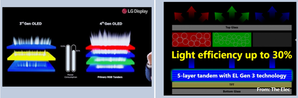
Large-size WOLED: Unlike FMM-RGB technology, WOLED achieves full-color display by vapor-depositing white OLED material and then using a color filter on top, bypassing the challenges of FMM in large-size applications. In recent years, LGD has continuously improved the brightness, viewing angle, and energy efficiency of WOLED panels by introducing "META Technology" (including microlens arrays and brightness enhancement algorithms). To date, LGD remains the only manufacturer in the world mass-producing large-size WOLED TV panels.

Source: LGD
Small and medium-sized POLEDs: POLED (Polymer Organic Display) is mainly used in smartphones, smartwatches, automotive displays, and high-end laptops. This technology uses traditional FMM technology and directly competes with Samsung Display. LGD is also constantly innovating in this field, such as developing Tandem (double-layer stacked) OLED technology, which is more durable and better suited for foldable devices.
In addition, LGD continues to invest in cutting-edge fields such as transparent OLED, and its products have been applied in various scenarios such as commercial display and transportation.
Currently, LGD is evaluating FMM-free technology. On the one hand, it hopes to explore the possibility of transforming its WOLED production line into an FMM-free RGB OLED production line with minimal equipment modifications, thereby improving its production line utilization and expanding its future potential development space.
Looking at the size products that JDI has invested in developing eLEAP technology in the past, including head-mounted display panels, wearable watch panels, laptop panels and large automotive panels, it is evident that the FMM-free technology, in theory, has the potential to cover all sizes of applications and even meet the ultra-high PPI specifications of head-mounted display panels, with the PPI limit theoretically lifted.
For LG Display (LGD), the FMM-less technology may complement its mature WOLED technology, allowing LGD to refine its product portfolio across various panel sizes. WOLED will continue to solidify its advantage in the mid-to-large-sized TV and monitor market, while the FMM-less technology, building upon POLED, could become a powerful tool for LGD to penetrate new markets such as laptops, automotive displays, medical professional displays, and even smaller-sized products.
FMM is approaching its "ceiling," and expectations for FMM-free OLEDs are rising . It is understood that in the manufacturing of mainstream small and medium-sized OLED panels, the key to determining screen resolution, color accuracy, and yield lies in how to accurately deposit tiny organic light-emitting materials onto designated locations on the substrate. FMM is a consumable core component in the OLED evaporation process, and its main function is to deposit RGB organic materials and form pixels during OLED production.
FMM (Fixed-Mesh Mask) is an extremely thin metal plate with micron-sized holes. As resolution and pixel count increase, the holes on the metal mask become finer and denser. A single metal mask can have approximately 20 million holes, making the manufacturing process quite challenging. Furthermore, each sub-pixel of each RGB color requires a different FMM and repeated vapor deposition processes.
As size and demand increase, FMM technology is gradually approaching its physical limits, resulting in a series of problems such as large precision limitations and low material utilization, which in turn affect the pixel density, brightness, and lifespan of OLED displays. The specific challenges are as follows:
Resolution Limits: Because FMM itself requires a certain thickness and frame support, it limits the fineness of the aperture and the arrangement density. OLED pixel density is difficult to break through the ceiling of 1000 PPI, which is a major obstacle for AR/VR devices that require ultra-high resolution.
"Shading effect" and material waste: The metal frame of the FMM will block part of the evaporation area, resulting in a limited aperture ratio (effective light-emitting area), which affects screen brightness and energy efficiency. At the same time, a large amount of organic material will adhere to the mask rather than the substrate, resulting in material waste and increased costs.
Large-size manufacturing challenges: As panel sizes increase, FMM (Film-Modified Metal Module) suffers from sagging and deformation due to gravity, leading to misalignment of the vapor deposition pattern and a significant decrease in yield. Therefore, FMM technology is currently mainly used for small and medium-sized panels, while large-size TV panels mostly employ WOLED technology and similar QD-OLED technologies.
Production cycle and cost: The design and manufacturing process of FMM is complex and expensive, especially for customized products and irregularly shaped screens, where the mold opening cost of FMM is high and the cycle is long.
Analysis shows that during the upgrade from generation 6 to generation 8.6, the development difficulty of FMM (Flat Metal Melting Machine) increased sharply, with color deviation and vapor deposition uniformity becoming key technical challenges. While Tandem (double-layer stacking) technology can improve product lifespan, its repetitive manufacturing process will lead to challenges in yield, thus affecting costs.

Against this backdrop, FMM-free technology based on semiconductor photolithography is gradually gaining market attention and anticipation. The core idea of this technology is to eliminate the reliance on physical "masks" for masking. Instead, it first deposits organic light-emitting materials over a large area on a substrate, and then uses photolithography processes, including exposure and development, to "carve" the organic material layer, ultimately forming the desired RGB sub-pixel pattern. Its main advantages are as follows:
High resolution: Because photolithography can achieve a precision far exceeding that of FMM, the pixel density can theoretically be increased to thousands or even tens of thousands of PPI;
High aperture ratio: Since there is no need for FMM as a shield, the aperture ratio can be greatly improved (e.g., JDI claims that its eLEAP technology has an aperture ratio of over 60%, which is twice that of traditional FMM). This means that under the same brightness, the driving current is smaller, which is conducive to extending the life of OLED and improving the "burn-in" problem; or under the same lifespan, higher peak brightness can be achieved.
Large size and free form: Photolithography is not limited by the size of equipment and related components, making it possible to manufacture larger OLED panels with arbitrary shapes.
Cost reduction and efficiency improvement: Although the initial equipment investment is high, in the long run, this technology can significantly reduce the waste of organic materials and eliminate the design, manufacturing and cleaning costs of FMM, which is expected to reduce the overall production cost.
Although this technology has not yet been verified, the industry believes that it has development potential in niche OLED panel fields, such as medium-sized panels for IT or automotive displays, which are suitable for small-scale mass production of advanced technology and are expected to become the main application areas for FMM-free OLED technology in the future.
Currently, FMM-free technology has attracted the attention of leading panel manufacturers in China, Japan, and South Korea. Companies such as Japan Display Inc. (JDI), Visionox (China), and Samsung Display Inc. (SDC) (South Korea) are actively developing related technologies. If the rumors are true, it means that LG Display has also entered this field.
The competitive landscape for FMM-less technologies has begun to take shape, and a new round of fierce competition has begun.
JDI: JDI was the first company to enter the field of FMM-free technology. In May 2022, it released eLEAP technology. Compared with Sony's W OLED based on white light and color filter at the time, the aperture ratio (the ratio of the light-transmitting area to the total area) of OLED displays produced by eLEAP technology can reach 60%.
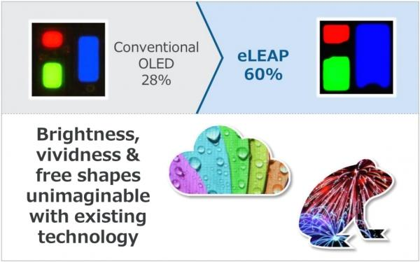
Image source: JDI
In 2022, eLEAP began shipping samples. In April 2023, JDI responded to customer demand and developed a 14-inch notebook product with a peak brightness of 1600 nits, three times that of JDI's previous OLED products. JDI stated that if eLEAP uses a series structure, the brightness can reach over 3000 nits. In October of the same year, JDI began trial production of eLEAP technology, and in April 2024, it achieved a significant breakthrough—a yield rate exceeding 60%, overcoming the main challenges on the road to mass production.
Beyond technological breakthroughs, JDI actively collaborates with other manufacturers to promote the commercialization of eLEAP technology.
In late 2024, JDI, Innolux, and its subsidiary CarUX jointly established the eLEAP strategic alliance to promote 32-inch OLED integrated automotive displays. Reportedly, their next-generation OLED "eLEAP" display technology offers double the brightness and triple the lifespan compared to existing OLED displays on the market.
However, in February 2025, JDI announced that due to long-term financial pressure, it would consolidate its production plants and abandon the self-production of eLEAP technology. Instead, it would seek to develop the technology with other strategic partners and entrust the production to them. Therefore, the future of eLEAP technology remains to be seen.
Visionox: Following JDI, Visionox released its FMM-free technology, ViP (Visionox intelligent Pixelation), in May 2023.
This technology utilizes semiconductor photolithography to fabricate pixel patterns, resulting in higher aperture ratios and lower IR drop. Characterized by independent pixels, it effectively suppresses growing dark spot (GDS) phenomena. Furthermore, it supports various pixel arrangements, increasing the AMOLED aperture ratio from the traditional 29% to 69% and pixel density to over 1700 PPI. When combined with Visionox's Tandem stacked devices, the device lifetime and brightness are 6 times and 4 times that of FMM AMOLED, respectively.

Source: Visionox
In December 2023, Visionox successfully lit up the first module of its ViP AMOLED mass production project, marking the successful completion of the ViP technology mass production process and a significant step towards mass production. In September 2024, Visionox's new G8.6 generation AMOLED production line (led by its joint venture Hefei Guoxian) commenced construction, and is expected to simultaneously introduce FMM and ViP technologies, targeting the medium and large-size market, with products covering applications such as tablets, laptops, and automotive displays.
In terms of intellectual property, Visionox has covered more than ten technical fields in its ViP technology layout, with a total of more than 500 patents. It has carried out a comprehensive technical layout around key elements such as pixel definition layer, isolation structure, independent packaging, and auxiliary cathode, forming multiple independent intellectual property technology combinations.
Samsung Display: Samsung Display (SDC) also began exploring new OLED panel manufacturing processes in 2023. In June 2024, according to South Korean media reports, Samsung Display purchased five US patents in the field of FMM-free OLEDs from the US company Orthogonal, including patents on "photolithographic patterning of organic electronic devices" and "color OLED displays with a larger aperture ratio".
Based on this, Samsung Display is reportedly purchasing non-FMM vapor deposition equipment from Applied Materials for evaluation in its R&D production line, indicating that Samsung is preparing for future technology iterations.
Samsung Display is focusing on quantum dot technology in its OLED technology roadmap. Unlike WOLED, QD-OLED technology uses a blue OLED light source to excite red and green quantum dot layers to directly generate the three primary colors of RGB, without relying on white sub-pixels, resulting in better color purity and brightness.
TCL CSOT: Printed OLED technology (IJP) is also an innovative FMM-free technology. This technology uses RGB light-emitting materials as inkjet materials, and directly patterns the ink droplets on the substrate by spraying them onto the designated position through the nozzle. The process is simplified, the material utilization rate is high, the material loss can be reduced by 30%, and it is not limited by large-size FMM.
Currently, TCL CSOT is the only panel manufacturer that has deployed printed OLED technology, primarily targeting mid-sized applications. Its t5 production line began trial production of a 21.6-inch 4K medical display at the end of last year. Building on this, TCL CSOT plans to advance the mass production of printed OLED consumer products on a quarterly basis. At this year's SID Display Week, TCL CSOT showcased a complete suite of printed OLED products, ranging from 6.5-inch mobile phone displays to 65-inch TV displays.
In summary, Visionox is making rapid progress in the field of FMM-free technology, actively advancing both technologically and in terms of production capacity. If the reports regarding Samsung Display and LG Display are true, and considering that OLED is considered a strategic direction at the national level in South Korea, Samsung Display and LG Display may also accelerate their related work in the future.
It is evident that a preliminary competitive landscape for FMM-free technologies has been established, and a new round of competition between China, Japan, and South Korea has begun.

Mid-size breakthrough: Players without FMM technology embrace a larger stage <br /> Currently, among all new display technologies, the competitive landscape of OLED is as follows: small-size OLEDs are far ahead, mid-size OLEDs are poised for a breakthrough, and large-size OLEDs are progressing slowly. In other words, mid-size OLEDs are currently the area where OLEDs have the potential to explode.
In the small-size segment, OLED has firmly established itself as the king of smartphones. According to data from the "AMOLED Industry Chain Report" and the "AMOLED Market and Technology Trends Report," OLED penetration in smartphones is projected to reach 61% by 2025. Furthermore, Apple has sparked a new wave of investment in next-generation OLED production lines, which is expected to drive more IT brands to adopt OLED panels in their products.
In the mid-sized display market, including notebooks (NBs) and mini-monitors (MNTs), OLED technology is still in its early stages, primarily facing challenges related to lifespan and cost. However, unlike the current situation with large-sized displays (which are experiencing slow growth due to cost and production capacity constraints), the mid-sized display market, encompassing notebooks, MNTs, tablets, and automotive displays, has become a fiercely competitive arena as consumers increasingly demand higher-end display performance.
In this round of competition, manufacturers in the industry chain have gradually made breakthroughs in materials and costs.
Materials: Upgrading Blue Light-Emitting Materials, Optimizing Aging Mechanisms of Luminescent Materials <br /> According to research, blue phosphorescent materials are rapidly becoming commercialized, and the combined development of TADF sensitization technology and high color gamut materials is gradually improving. This not only retains the advantage of TADF's 100% internal quantum efficiency but also compensates for the shortcomings of traditional fluorescent materials in luminescence efficiency, resulting in a significant improvement in performance and stability. Furthermore, with the publication of more and more research, the aging mechanisms of luminescent materials are becoming increasingly clear.
Cost: Domestic manufacturers' breakthroughs in materials accelerate cost optimization . Domestic manufacturers have made breakthroughs in key OLED technology materials such as UTG and FMM. For example, UTG has broken Schott's monopoly, developing master wafers of 30μm or even thinner for processing. FMM has now entered mass production and verification on the G6 production line. These breakthroughs will help improve costs.
Thanks to breakthroughs in materials and cost optimization, OLEDs are gradually extending into medium-sized applications such as foldable laptops and automotive displays. However, the competition for brightness and cost remain the core variables in market competition.
In addition, the mid-size OLED market is at a critical stage of technological innovation and cost control. Besides high-generation production lines and new vapor deposition technologies, the accelerated development of FMM-free technology will also help improve the performance of OLED products, control costs, and help OLED open up the mid-size OLED application market.
According to data, in 2025, the penetration rate of OLED in the laptop market reached 4.5%, showing steady growth. At the same time, it is estimated that the shipment volume of OLED displays will increase by 83% year-on-year in 2025, and the overall display market penetration rate will rise to 2%, with the potential to challenge 5% by 2028.
The expansion of the OLED market also means that FMM-free technology has a larger stage. Manufacturers who have invested in FMM-free technology are expected to use this opportunity to promote the implementation and commercialization of the technology, thereby turning it into a driving force for revenue growth.
Conclusion <br /> Regardless of whether LGD will invest heavily in FMM-free OLED technology, this technology continues to receive attention and its prospects are bright. However, it is still in the early stages of development, and several challenges need to be overcome before mass production can be achieved. Analysis suggests that, taking Visionox's ViP technology as an example, the complexity of the process, requiring multiple masking and etching steps, poses a challenge to yield. As for printed OLED technology, once mature, it is expected to be applied to higher-generation production lines, but inkjet precision and material uniformity still require further breakthroughs. (Text: Chen Jiachun)


